Russia to Establish an Advanced Electron‑Beam Lithography Laboratory
A new federal initiative will expand access to lithography systems, accelerate problem‑solving in microelectronics, and launch a domestic scientific‑instrumentation program

A Strategic Push for Microelectronics
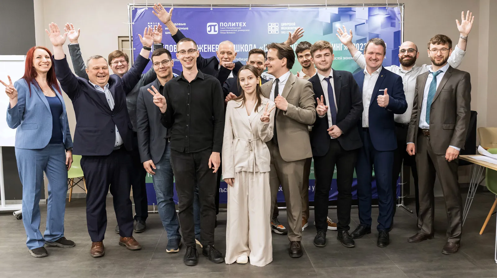
Russia’s Ministry of Science and Higher Education will support the development of electron‑beam lithography for microchip production in 2026, Minister Valery Falkov announced at President Vladimir Putin’s meeting with participants of the Fifth Congress of Young Scientists. To enable this progress, the country will create an advanced engineering school or a dedicated youth laboratory specializing in electron‑beam lithography.
Falkov explained that the government has two viable paths: expanding the existing network of advanced engineering schools or establishing new youth laboratories, which have already proven effective.
Meeting the Growing Demand
Alexander Barulin, a researcher at the Laboratory of Controlled Optical Nanostructures at the Center for Photonics and Two‑Dimensional Materials of the Moscow Institute of Physics and Technology, urged the President to support this initiative. He emphasized that the scientific community needs broader access to lithography systems because existing installations are overloaded.
According to Barulin, increasing the number of systems in research centers would allow scientists to solve engineering and research tasks faster. Another path forward, he suggested, is launching a national scientific‑instrumentation program aimed at developing a fully domestic electron‑beam lithography system.
Why It Matters
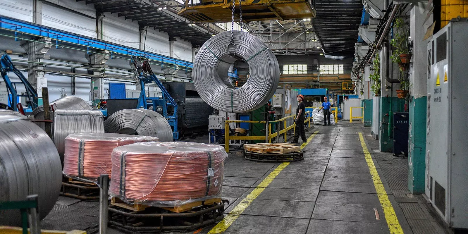
Expanding access to electron‑beam lithography directly strengthens Russia’s semiconductor ecosystem. With more systems available, research workflows speed up, development cycles shorten, and teams can prototype advanced microstructures without long queues or dependence on foreign equipment. A successful domestic lithography project would also reduce import reliance and lay the foundation for next‑generation scientific tools built entirely within the country.