Four Megapixels of Sovereignty
Seventy years after its founding, Russia’s Central Research Institute Elektron is marking a milestone by moving from space-era imaging to next-generation sensors, chips, and photonic systems that underpin industrial automation, energy exploration, and scientific infrastructure.

At the Technological Front Line
The Central Research Institute Elektron, a flagship of Russian photoelectronics, marks its 70th anniversary in 2025. Over seven decades, the institute has become a pillar of national science and industry. Its vidicons captured Yuri Gagarin’s historic spaceflight in 1961, and in 2015 more than 16,000 photomultiplier tubes produced by the institute contributed to the detection of the Higgs boson. Today, the institute remains at the cutting edge, delivering key projects aimed at technological self-sufficiency.
A Digital Eye for Machine Vision
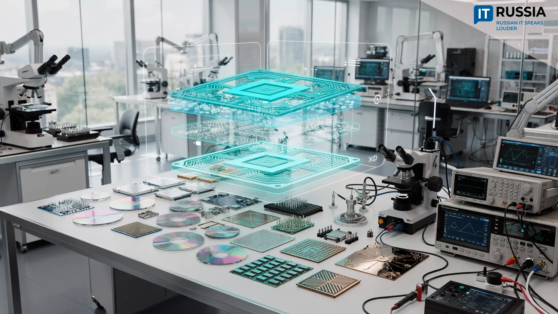
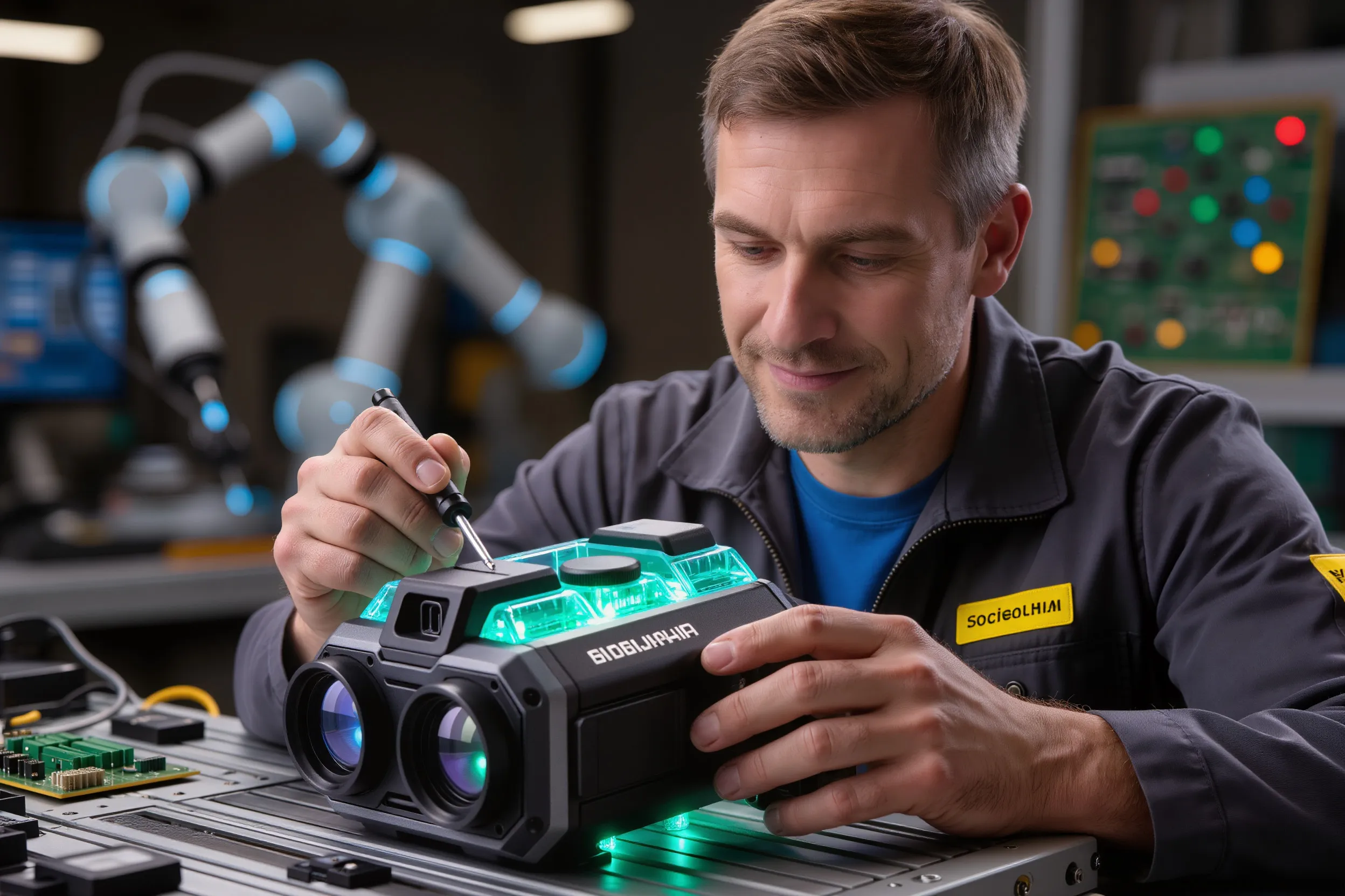
One of the institute’s landmark achievements is the creation of Russia’s first CMOS image sensor with a resolution of 2048×2048 pixels, or four megapixels, fully designed and manufactured domestically at the Mikron facilities in Zelenograd. The uniqueness of the solution lies in its entirely Russian lineage, from circuit design to the finished chip. Each pixel is physical rather than interpolated, ensuring high image clarity even under digital zoom.
This type of sensor can serve as a foundation for machine vision systems, optoelectronic complexes, industrial automation, robotics, and autonomous vehicles, where precision and minimal image latency are critical.
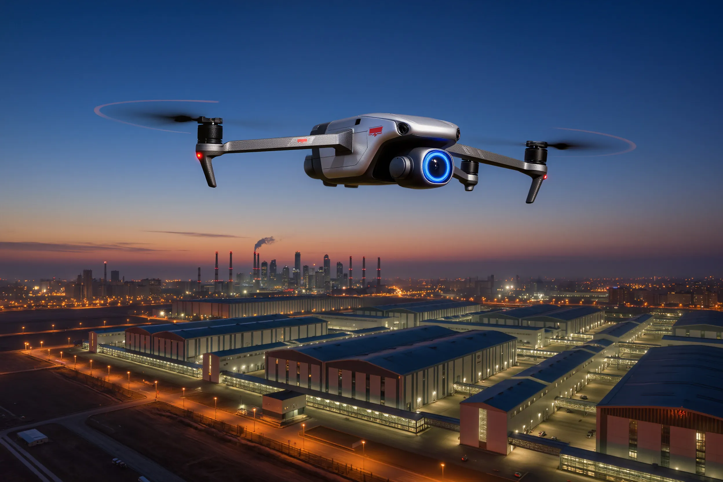
At the same time, researchers at the institute are developing a compact, ultra-high-speed CMOS sensor capable of up to 450 frames per second. The device is tailored for drones and robotic platforms, where ultra-low image latency is essential for navigation and control.
The Fifth Element of Photoelectronics
Another breakthrough direction is a fifth-generation electron–optical converter. Unlike traditional systems, it detects photons and then converts them directly into electrons, dramatically increasing sensitivity and efficiency. By eliminating phosphors and optical chains, engineers have created a compact yet high-performance device adaptable to ultraviolet, visible, and near-infrared ranges.
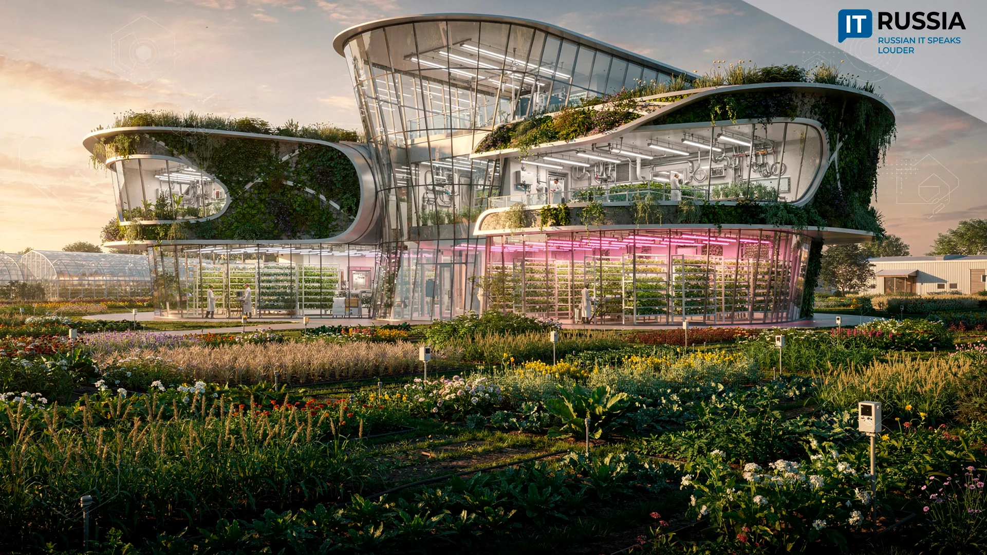
The new-generation converter is designed for use in measurement and inspection systems, nondestructive testing, agricultural technologies, and other industrial sectors where reliable sensing is required under low-light or UV and IR conditions.

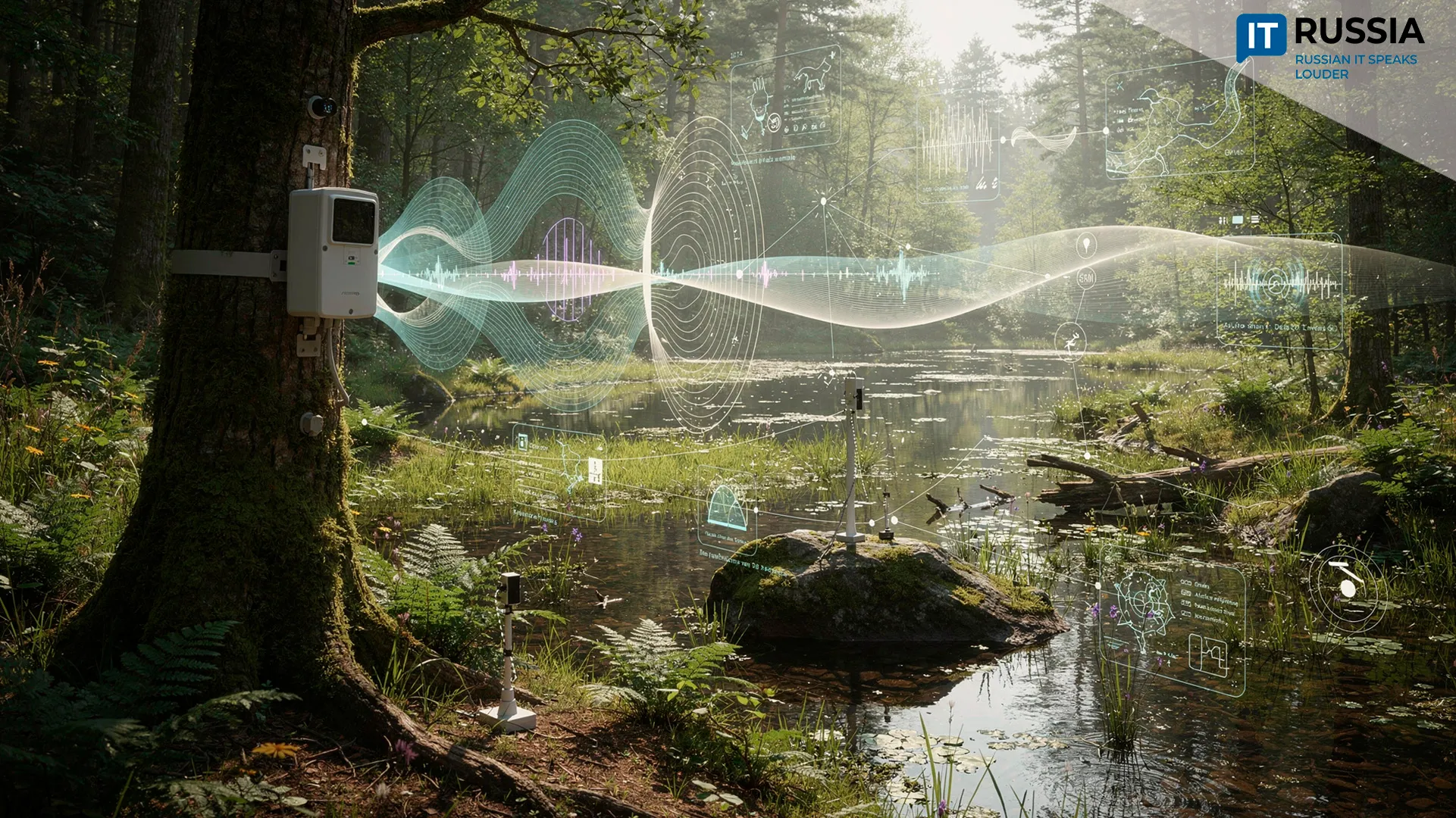
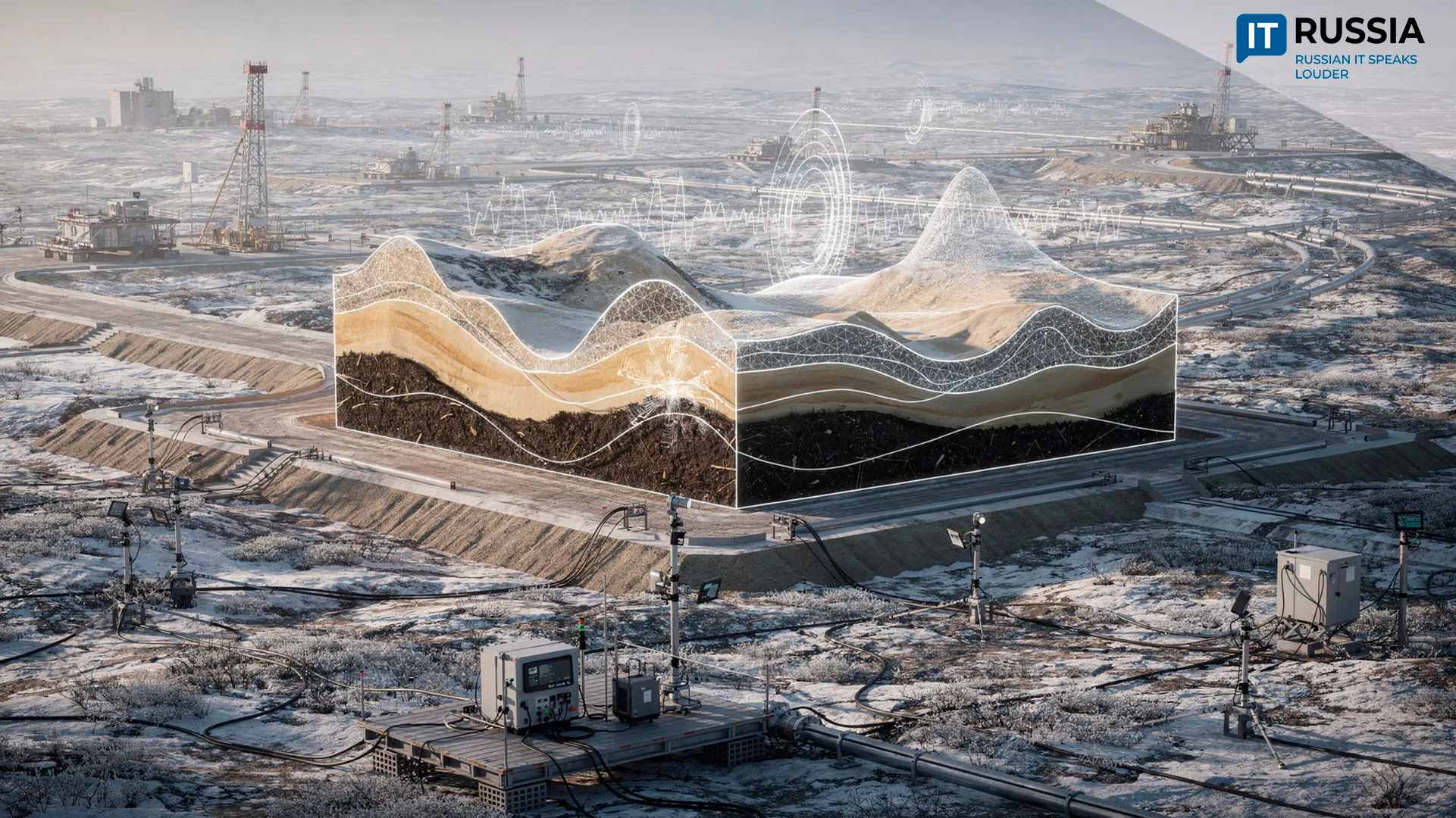
Electronic Eyes Underground
Equally important are high-temperature, miniature photomultiplier tubes developed for geological exploration. The first experimental samples were manufactured in November 2025 and have already demonstrated performance comparable to Japanese counterparts. These devices can operate in boreholes at temperatures up to 160 degrees Celsius and pressures of thousands of atmospheres, detecting faint light flashes during neutron logging.
Based on the incoming data, operators at the surface can determine the composition and structure of underground formations in real time. Serial production is planned to begin after field trials scheduled for December 2026.
From Microelectronics to Laser Eyes for ITER
Over the past decade, Russian photonics has achieved notable progress across a wide range of applications, from microelectronics to participation in global scientific projects. In 2020, the company Fistekh was founded in Russia, becoming the first to develop domestic photonic integrated circuits with bandwidths of up to 22 gigahertz.
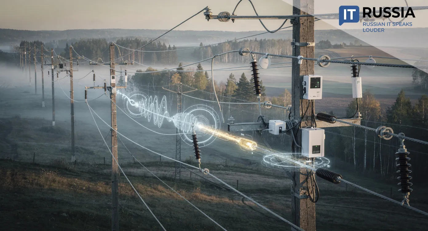
In December 2025, serial production of these circuits was launched at the Moscow Photonics Center, with capacity reaching up to 500,000 chips per year, covering as much as 10% of domestic demand. These components transmit data at the speed of light without electromagnetic interference and are expected to form the backbone of Russian 5G networks, the Internet of Things, data centers, and telecommunications infrastructure.
At the same time, Russian scientists are applying photonic technologies to fundamental research. Specialists at the Budker Institute of Nuclear Physics of the Siberian Branch of the Russian Academy of Sciences have developed a unique optical system to control the geometry of blind cooling channels in diagnostic modules of the international thermonuclear reactor ITER. Using a laser tracker and optical gauges, the system delivers precision measurements in environments where conventional methods fail. This technology ensures safe reactor operation under extreme temperatures and radiation.
Taken together, these developments show that Russian photonics is advancing steadily across both applied and scientific domains, demonstrating its ability to support technological sovereignty while contributing to global research.

Russian Photoelectronics Preparing for a Breakthrough
The developments at the Central Research Institute Elektron are more than isolated scientific achievements. They form the backbone of strategic import substitution in critical industries. Looking ahead, CMOS sensors, fifth-generation electron–optical converters, and specialized detectors could find demand in export markets, including industrial optics, surveillance systems, and specialized electronics.
To reach that stage, however, significant challenges remain. Production volumes must be scaled up, parameter stability ensured, and manufacturing infrastructure modernized to compete with global players such as Sony, Teledyne, and Canon. By 2030, mass production of Russian image sensors and electron–optical converters is expected to begin, followed by the first commercial contracts and later serial output of high-speed matrices and high-sensitivity detectors. This would mark an important step toward strengthening Russia’s position in the global high-tech market.