Memory for the Future: Russian Researchers Take a Step Toward Next-Generation Electronics
Researchers at the Moscow Institute of Physics and Technology report a breakthrough in ferroelectric memory development: experimental samples have withstood more than 100 million rewrite cycles, orders of magnitude beyond typical flash memory performance.
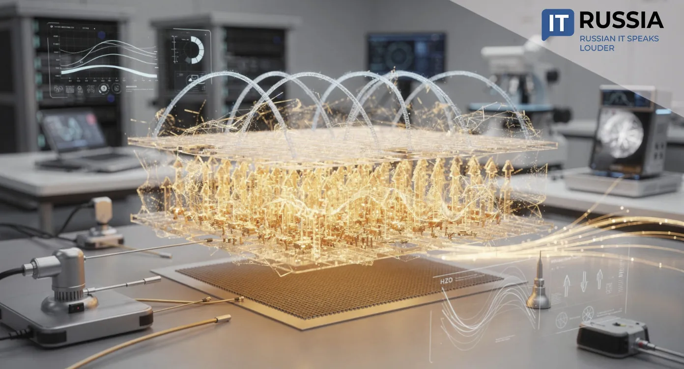
The MIPT team has demonstrated record endurance for ferroelectric memory, reaching 100 million rewrite cycles. This marks an important milestone for energy-efficient electronics that could reshape applications ranging from cardiac pacemakers to artificial intelligence systems.
What Is Ferroelectric Memory
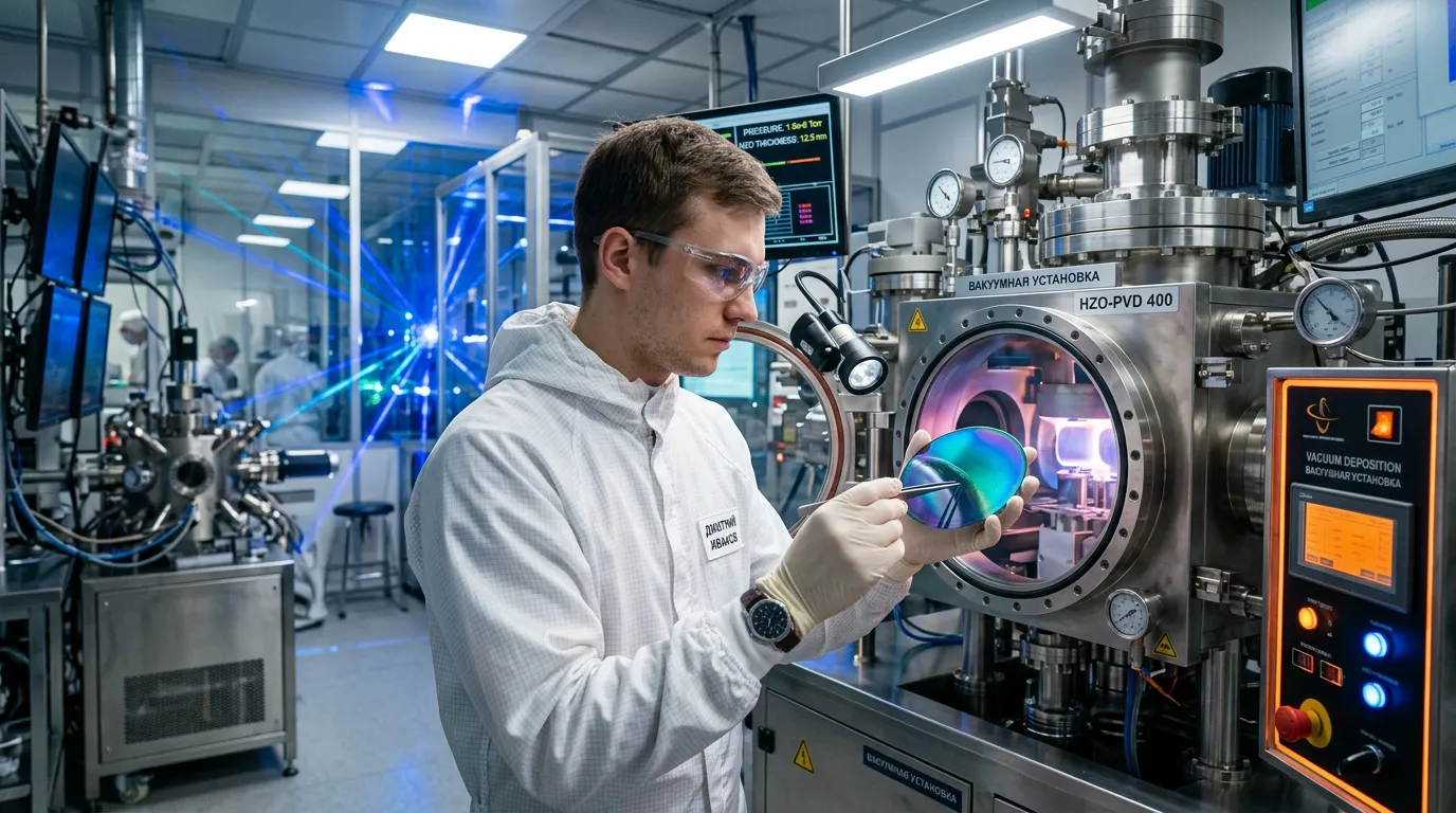
Conventional flash memory used in smartphones and USB drives degrades over time, with cells wearing out after tens of thousands of write cycles. Ferroelectric memory based on hafnium–zirconium oxide (HZO) operates differently. It relies on the material’s ability to retain polarization without continuous power. That approach offers high speed, low energy use, and, critically, far greater endurance.
A central scientific challenge lies in balancing competing factors. Thinner films reduce operating voltage and improve energy efficiency. At the same time, they increase leakage currents and reduce reliability. The MIPT team appears to have identified a viable solution to this trade-off.
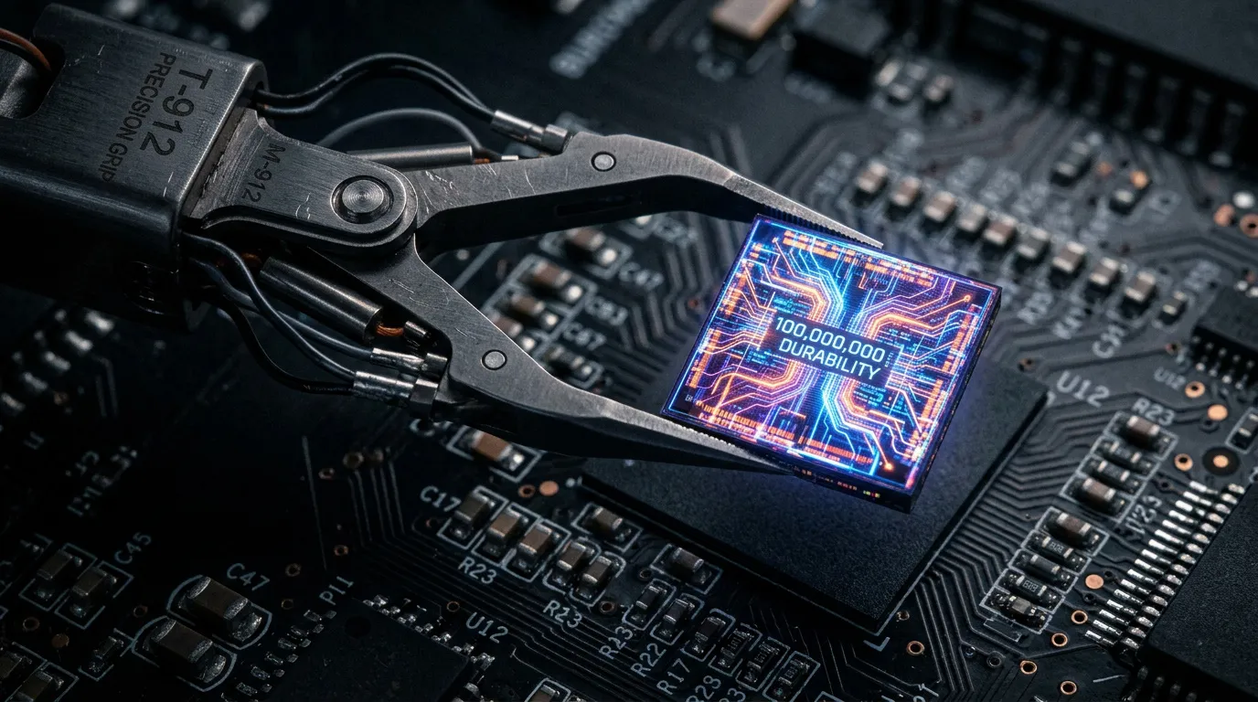
A Breakthrough in Numbers: 100 Million Cycles
Results published in Journal of Alloys and Compounds, Physical Review Applied, and Applied Physics Letters show that HZO-based memory can sustain 10⁸ rewrite cycles without performance loss. By comparison, conventional NAND flash typically withstands between 10³ and 10⁴ cycles.
This is not yet a market-ready chip but a fundamental scientific result. The researchers have not simply extended device lifetime. Instead, they have advanced understanding of physical processes in ultrathin films, which opens a pathway to targeted optimization.
Why It Matters for Russia and Beyond
For Russia’s microelectronics sector, this work represents a strategic foundation. As global supply chains remain uncertain, building domestic expertise in materials, memory architectures, and neuromorphic computing is increasingly tied to technological sovereignty.
For end users, the benefits may not be immediate, but the trajectory is clear. More autonomous medical implants, energy-efficient data centers for AI, and robust electronics for industry and transport could follow. MIPT highlights pacemakers, neural interfaces, and edge devices among priority applications.
From Laboratory to Production: What Comes Next?
Translating laboratory results into scalable products remains complex. It requires wafer-level reproducibility, compatibility with CMOS processes, stability under temperature and radiation, and the development of controllers and testing methods.
However, a research foundation is already taking shape. Over the past five years, MIPT teams have published a series of studies, including work on flexible memristors, suppression of the wake-up effect, and analysis of leakage currents in nanofilms. Taken together, these efforts suggest a coordinated research program rather than isolated advances.

Outlook: Two Development Tracks
In the coming years, this field is likely to evolve along two main tracks. The first focuses on materials and device physics, including improving data retention, mitigating degradation, managing phase transitions, and achieving reproducible structures. The second centers on system architecture, with applications in neuromorphic computing, edge AI, medical devices, and embedded electronics, where non-volatility and instant startup are critical.
If Russian researchers sustain publication momentum and strengthen collaboration with manufacturing centers, this work could contribute not only to academic research but also to the development of applied microelectronics globally.
This is not a story about a “super flash drive” arriving tomorrow. Instead, it reflects sustained efforts at the intersection of physics, materials science, and engineering that are gradually reshaping the technological landscape.